
Table of Contents
Both GDDR6 and HBM2 are types of memory that enable processors to perform better in a wide variety of applications due to their high memory bandwidth. In this article, we compare the architecture, performance (including Bandwidth and speed), and price differences between the two types of memory.
Short Definitions of GDDR6 and HBM2
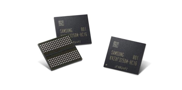
GDDR6 is an abbreviation for Graphics Double Data Rate type 6. It’s a type of synchronous graphics RAM with high bandwidth, designed for high-performance applications such as graphics cards and game consoles.
HBM2 stands for High Bandwidth Memory (v2) and is another type of memory commonly found in graphics cards, as well as 3D-stacked DRAM chips. It makes use of stacked DRAM dies which are connected with microbumps and through-silicon vias.
Read Related Article: CPU Cores vs Threads
Video Comparison of GDDR6 VS HBM2 by Semiconductor Engineering:
Architecture of GDDR6
The architecture of GDDR6 is an interesting combination of features commonly found in GDDR5 and GDDR5X, as well as some from HBM2. However, it does make some notable improvements.
For starters, GDDR5 and earlier versions only supported a single 32-bit channel with one command/address bus and one 32-bit data bus. This was simple and very straightforward. With GDDR5X, there was a single true 32-bit channel, but you could split that into 2 16-bit pseudo-channels. This configuration didn’t come with a lot of flexibility because you had both read and write operations within the same row.
GDDR6’s two-channel architecture
GDDR6 comes as a single chip, but that chip actually behaves like two DRAMs that are completely independent. They each have their own command/address bus, as well as their own 16-bit data bus. This is a benefit, because the more channels you have in a system, the more chances the memory controller has to manage the DRAMs. Which helps to avoid large stalls that usually happen because of page activation limits or page refreshes.

Another excellent benefit of GDDR6’s two-channel architecture is that it counteracts the consequences of the 16-cycle burst length. If you have a burst length of 16 with a 32-bit wide bus, the resulting transaction atom is 64 bytes. Numerous architectures, both GPU and CPU, make use of 32-byte transaction atoms. If you split up the DRAM in two channels that are independent and 16 bits each, you get a 16n prefetch, and still keep a transaction size of 32 bytes.
QDR and DDR
Up until GDDR5X, DRAM was DDR (double data rate). The data bits would change at the rising and the falling edge of the word clock (WCK). With GDDR5X, we saw the introduction of QDR (quad data rate). Data would toggle at four times the WCK frequency, or twice as fast as DDR. GDDR5X had support for both QDR and DDR, but the DRAM would run at half the speed during the DDR mode. It was only there as a power saving option.
With GDDR6, you now have a choice between QDR and DDR at full speed. The specifications don’t really require a vendor to support both, so you’re basically getting two standards. As an example, if you have a GDDR6 DRAM at 14 Gbps, WCK will run at 3.5 GHz for a QDR device and 7 GHz for a DDR device. In both situations, the command and address clock, as well as the command and address lines themselves, run at 1.75 Gbps. In the specifications, there was also a mention of ODR (octa data rate), but no further details were uncovered, so this may come in the future.
Architecture of HBM2
HBM, or high bandwidth memory, provides higher bandwidth while also utilizing less power. Therefore, it has a different architecture than GDDR. All the DRAM dies (up to eight) are stacked, as well as an optional base die which contains a memory controller. They’re interconnected with through-silicon vias (TSV) and microbumps, as mentioned earlier. The way HBM works is similar to the Hybrid Memory Cube that was developed by Micron Technology but is incompatible with it.
Compared to other DRAM memories, the HBM memory bus is very wide. If you have four DRAM dies in the stack (4-Hi), there are two 128-bit channels for each die, which totals 8 channels and 1024 bits. Therefore, if you have a GPU with four 4-Hi HBM stacks, the total memory bus width is 4096 bits. As a comparison, the bus width for a GDDR memory is 32 bits and 16 channels for a GPU that has a 512-bit memory interface.
 Interposer
 Interposer
Considering there are a lot of connections to the memory, this requires a new method of connecting the memory to the GPU. Both AMD and Nvidia have made use of interposers, which are purpose-built chips, to achieve this. The interposer also requires that the memory and processor are physically close, which also reduces the memory paths. However, the fabrication of a semiconductor device is much more expensive than the manufacture of PCBs, which adds to the cost of the final product.
The DRAM for HBM is tightly coupled to the host computer die, using a distributed interface. This interface is actually divided into channels that are completely independent of one another, and they’re also not necessarily synchronous to each other. To achieve a high-speed operation while keeping the power consumption low, the HBM DRAM makes use of a wide-interface architecture. There’s a 500 MHz differential clock, and each channel interface has a 128-bit data bus which operates at DDR data rates. While the initial version supported transfer rates of 1 GT/s (gigatransfer per second), HBM2 increases this up to 2 GT/s.
Performance
When we’re only discussing performance, limiting things to only the memory type would be a mistake. Both GDDR6 and HBM2 are made in a different way, and they excel in different areas. For example, the high bandwidth of HBM2 is ideal in situations such as AI and advanced computing. This is why we’re seeing it in data center GPUs, such as Nvidia’s Tesla V100, where the cost consideration is less important. On the other hand, GDDR6 can offer a lot of the same performance, albeit with higher power requirements, but at a lower price. This makes it much more accessible for the everyday user, hence we’re seeing it in commercial graphics cards.
As far as gaming goes, both types of memory found their way in gaming graphics cards. However, we couldn’t say that one type of memory is better than another for gaming because there are a lot of other factors that come into play. Things such as bus width, base clock, and boost clock all matter, and you can find graphics cards with identical memory types performing differently from one another due to other factors being different. There is one advantage that HBM2 has here, even with the higher cost. The fact that it has a lot more bandwidth means that you’ll get better performance and less latency.
 Price (Production Cost)
 Price (Production Cost)
This is a section where GDDR6 takes the win by a large margin. To begin with, HBM2 is only in its second iteration and is not nearly as widespread as GDDR in terms of fabrication. The additional silicon interposer of HBM2 which gives electrical connectivity to the SoC is first and foremost, a design complexity. Solving this complexity is costly. Then, you have the fact that a semiconductor device is much more expensive to produce than a PCB, which adds even more to the cost.
As a result, the GPUs that would offer comparable results to their GDDR6 counterparts are significantly more expensive if they use HBM2. HBM2 does introduce a lower power consumption as well, but the production and implementation costs rules the price battle in favor of GDDR6.
Wrapping things up – which one is better?
In their current iterations, we couldn’t say which type of memory wins. There are tradeoffs with both types, and it’s merely a matter of which one is more acceptable to the end user.
Starting things off with the per-pin data rate, GDDR6 comes in with a much higher 16 Gbps, compared to HBM2’s 2 Gbps. The fact that there are no additional chips to manufacture also helps keep the costs down, which is always welcome.
On the other hand, due to the fact that it’s a stacked memory, the relative area of the PHY controller is much smaller for HBM2, with GDDR6 taking up as much as 1.5-1.75 x the area of HBM2’s controller. This also means that GDDR6 consumes 3.5-4.5 x the power when compared to HBM2. At the end of the day, it is up to the GPU manufacturers to choose which kind of memory fits their GPU’s intended use better and implement it in their graphics cards.
Read Another Article: Is MT/s the same as MHz?